



EDA Agent Connector
EDA Agent Connector
zhoushoujian546EDA Agent Connector
让 AI Agent 替你画板子。 这是 easyeda-agent 系统在 EasyEDA(嘉立创EDA专业版)内的社区连接器:配合本地 easyeda CLI/daemon 与 Agent Skill,通过官方 API 在真实编辑器里完成选型、放置、连线、方框标注与校验。
Skill / CLI -> Go daemon -> EDA Agent Connector -> 官方 eda.* API
一行看懂:Skill 描述专家工作流,Go CLI/daemon 提供有类型、可观测的动作与校验,本连接器把这些 typed actions 桥接到官方 eda.* API——它是整个系统中唯一直接调用 eda.* 的组件,每一步操作最终都落在嘉立创自己开放的插件能力上。
- GitHub 仓库:https://github.com/zhoushoujianwork/easyeda-agent
- 最新 Release:https://github.com/zhoushoujianwork/easyeda-agent/releases/latest
效果演示
门禁控制板示例:本地数据 → SCH Apply → 真实原理图
器件、物理引脚、稳定网络 ID 和 NC 保存在本地连接图中。Agent 依据实测引脚几何计算
功能 Lib 内的器件位置、方向和连线,再组合页面,通过 sch apply 顺序写入 EasyEDA
并回读核对,保留原位号与器件身份。
23 个器件 · 165 个物理引脚 · 28 个网络 · 2 页原理图
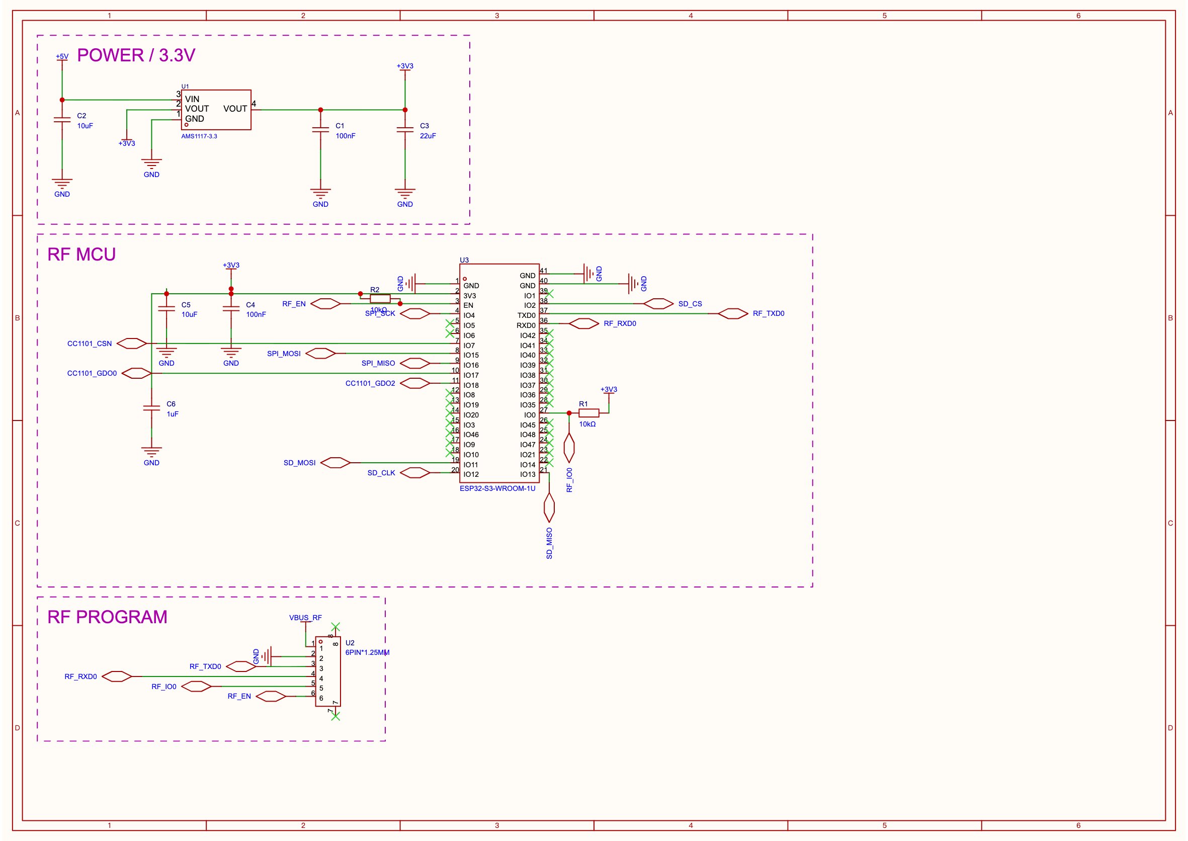
电源、RF 主控和下载接口分别组成 Lib;外围电路按引脚方向连接,端口长短错落。
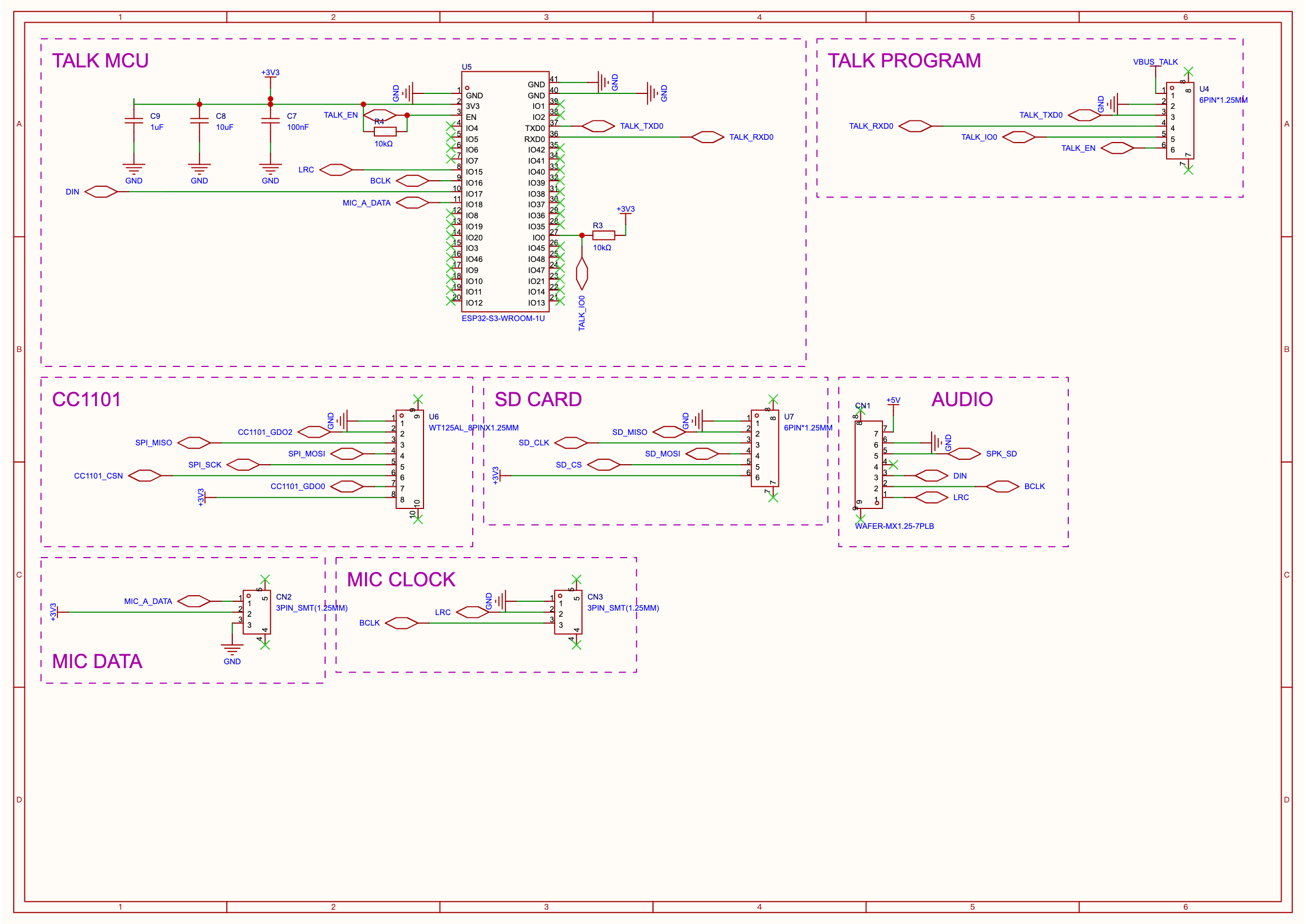
对讲与外设按 Z 字阅读顺序排列,每框随内容独立收紧并保留内边距,标题利用上方或下方空档。
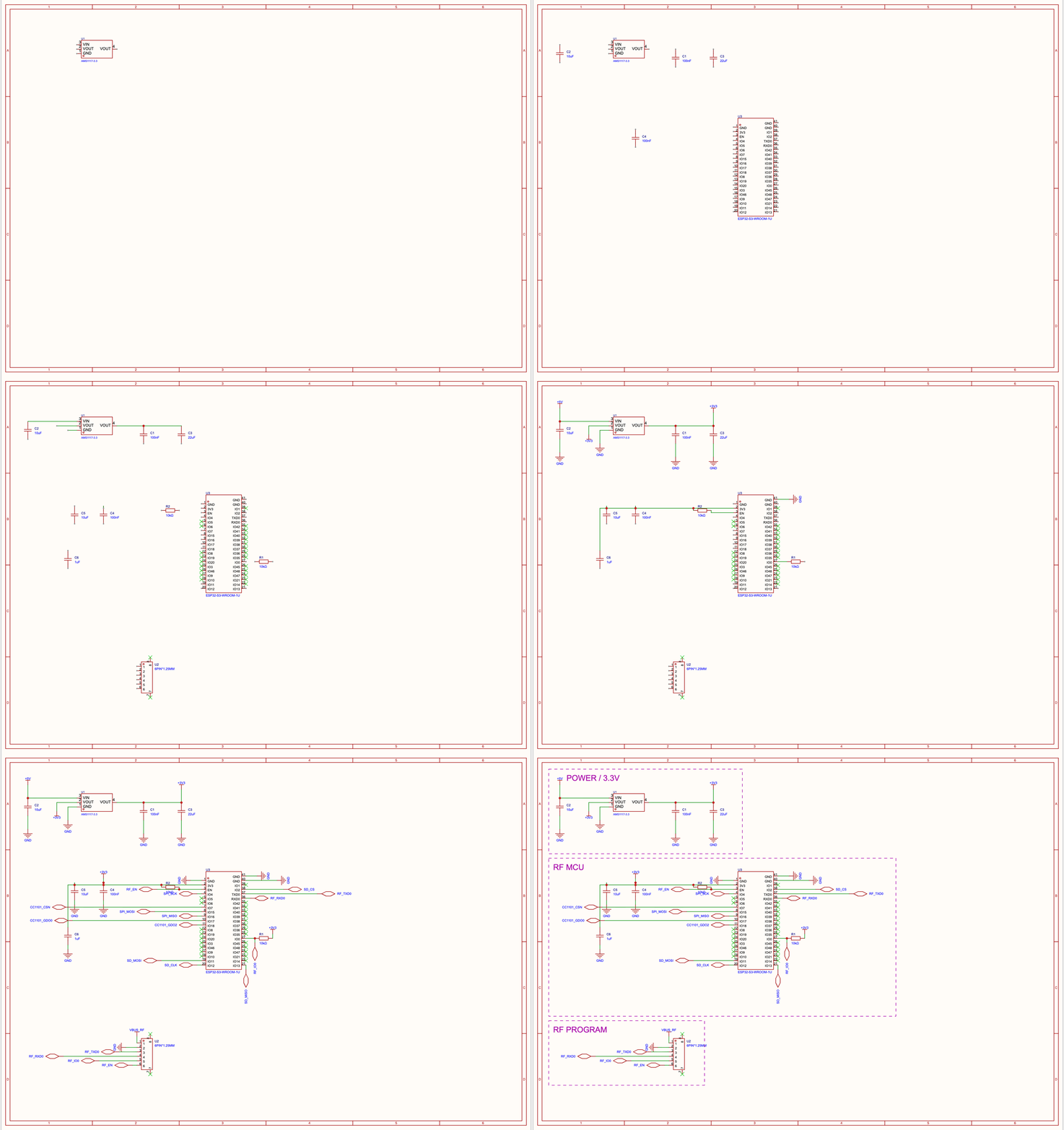
动图使用电源与 RF 主控页实际 Apply 捕捉的 12 张关键阶段导图,加速播放;静图源自 EasyEDA 官方导图,展示名称已匿名化。 录制方法见 Apply 动图捕捉。 两页布局与连接检查均为 0 错误、0 警告;官方 DRC 仍有 3 WARN,严格门禁未通过,部分文字避让仍待完善。 验证范围见 1.4 发布与验证。
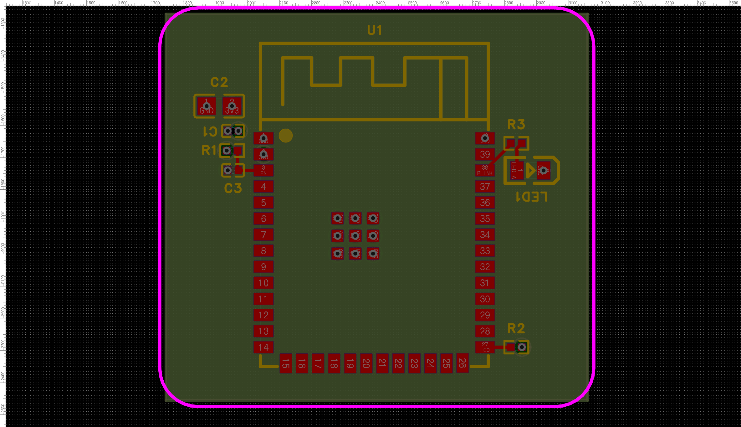
历史 PCB 案例:ESP32-S3 四层板
以下为独立的 ESP32 回归板案例:自动布局、板框贴合、铺铜、丝印,在真实画布上执行并回读校验。
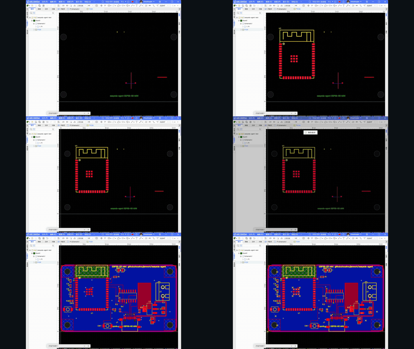
由 agent 驱动 PCB 流程产出的 ESP32-S3 板:自动布局 → 板框贴合 → 规则感知布线 → 4 层电源平面 → 丝印碰撞避让。历史验证记录见 完整案例。
1.4 数据驱动原理图
- 数据 → Lib compose → SCH Apply:在 canonical 数据中维护器件、引脚、网络与 NC,先设计 Lib 局部几何,再离线组合单页,通过顺序队列调用官方 API 并回读验证。
- 身份与显示分开:稳定器件 ID 用于数据绑定,合法数字位号保持原样,功能名称存 Role。
- 紧凑布局与方框:从左上向右按 Z 字排列,每框按内容独立收紧并保留最小内边距,同行顶齐,下一行按本行最大高度推进;粉色虚线框配 0.2 inch 标题,优先利用电路上方或下方空档。
版本与资产以 GitHub Release 为准。组合器使用已设计的模块几何, 不自动推导任意外围电路、分页或删除源页。构建步骤、已完成验证和未完成项见 1.4 发布与验证。
已支持能力概览
原理图
- 器件与库:从立创/LCSC 库按 uuid 放真实器件、换型号、符号/封装重绑、C 号确定性解析;库优先,手绘符号只是兜底。
- 连线:
connect/autoconnect(打分器自选方向,碰撞/穿件/图签全几何成本)、netflag/netport 自动补偿平台旋转存储的坑、成对删除。 - 布局与转换:
sch compose从已设计的 Lib 数据计算单页布局;sch apply顺序执行规划队列;sch frame apply/check生成并核对方框与标题。 - 校验与导出:Apply 后逐脚/网络/NC/几何回读,四阶段门禁(layout-lint → check → bridge-check → drc)、跨页网名审计、
sch read、BOM 导出(自动补 LCSC C 号)、网表导出、页面导图 SVG/PNG/PDF。
PCB
- 布局:新建板并绑定原理图、模块感知自动布局(间距规则感知)、板框贴合/圆角、布局质量与可布性评分、丝印位置感知避让重排、自由丝印字串(板注/LED 极性标记)。
- 布线与铜:启发式短线布线(规则感知线宽、障碍感知)、铺铜/禁铺区/过孔缝合、4 层电源分配(GND 内电层 + 电源平面 + 焊盘过孔缝合)、挖槽。
- 叠层与制造:铜层数与内层类型设置、读取板子实时 DRC 规则并全链路遵循(缺失时回退 JLCPCB 工艺参考)、DRC/
pcb check、Specctra DSN 导出/回导(对接外部 Freerouting)。
基础设施
- Typed action 协议:
--help自描述、动作目录可枚举,结构化输入输出,AI 每一步可观测、可验收、可回放。 - 连接器自愈重连看门狗(daemon 重启/窗口后台都能自动回来)、daemon 防抖自动保存、审计日志、窗口内非阻塞 toast 播报进度。
debug.exec_js用于任务范围内的临时调试。
完整能力清单与路线图见 FEATURES。
连接器本身做什么
这是一个真实可打包、可导入的 EasyEDA Pro 扩展,刻意保持很薄:
- 本地 WebSocket 传输:默认连接固定端口
60832、握手、注册、上下文同步、心跳、自愈重连; - typed action 分发:把 daemon 下发的结构化动作映射到官方
eda.*调用; - 结果序列化:执行结果、警告、错误、上下文回传 daemon;
- 产物传输:截图、BOM、网表等二进制结果编码回传。
真正的工作流、校验、确认、产物处理和多步编排都在 Go CLI/daemon 与 Skill 层完成——所以必须配套本地 easyeda CLI/daemon 一起用,单装本插件没有任何效果。
安装与开始
1. 装本连接器(两条通道任选):
- 在本市场页面点击「安装」——平台可原地自动更新,最省心;
- 或从 GitHub Release(https://github.com/zhoushoujianwork/easyeda-agent/releases/latest)侧载
easyeda-agent-connector.eext——与 CLI 严格同版。
2. 装 CLI/daemon + Skill(一行脚本,自动检测 Claude Code / Codex 并装好 Skill):
curl -fsSL https://raw.githubusercontent.com/zhoushoujianwork/easyeda-agent/main/install.sh | bash
3. 在 EasyEDA 中确认三件事:
- 已安装本连接器(市场安装或
.eext导入); - 已开启「允许外部交互 / Allow external interaction」——否则连接器的 WebSocket 连不上本地 daemon;
- 已启动本地 daemon(
easyeda daemon start),easyeda health能看到已连接窗口。
之后升级不必再跑脚本:easyeda update 一键升 CLI + Skill;easyeda update --check 只读三方(cli / skill / connector)版本对齐表。
版本配套约定
CLI/daemon、连接器与 Skill 遵循同一版本号。三者需配套安装,并运行开启外部交互的 EasyEDA Pro;EasyEDA 应用使用自身版本号。落后的连接器会被 easyeda daemon health 标成 stale。两条安装通道的取舍:
- 市场版:平台可原地自动更新,最省心;但市场无发布 API,每版需人工重新提交,上架版本可能滞后于 CLI。
- GitHub Release 侧载版:与 CLI 严格同版,需严格版本对齐时以它为准;代价是无原地自动更新,升级需手动卸载旧版再导入。
导入更新后需完全退出并重新启动 EasyEDA,已经打开的窗口可能仍运行旧连接器代码。
完整上手、版本对齐与升级注意事项见 快速开始。
更名说明(2026-08)
应市场管理规范要求,本插件显示名改为 EDA Agent Connector。内部包名与 uuid 均保持不变,同一条目重新上传——已装用户的原地自动更新不受影响,无需任何操作。
链接
- GitHub 仓库(架构、路线图、能力矩阵、实战案例):https://github.com/zhoushoujianwork/easyeda-agent
- Releases(严格同版
.eext+ CLI 各平台二进制):https://github.com/zhoushoujianwork/easyeda-agent/releases - 完整实战案例:一份需求文档 → ESP32-S3 四层板
MIT 许可,欢迎 star 与共建电路块库(一次贡献,署名可追,永久收益)。
Changelog
[1.9.1] - 2026-10-11
- 修复 DSH Git 插件安装时缺少
index.js的分发缺陷(#274);入口仅导出无副作用的 Cordisapply,MCP 与 Skill 由 bundle patch 加载。 - 根包声明 MCP SDK,分发清单仅包含入口、patch、MCP 源码与公开 Skill,Git 安装无需另行安装嵌套依赖。
- Windows、macOS、Linux CI 覆盖实际 npm tarball 安装、MCP 握手与离线目录发现;缺少缓存元数据时允许联网,不声明严格断网安装。
- macOS 独立环境验证 DSH CLI 0.1.5-rc.1(MCP/Skill 模块解析为 rc.3)的真实 Git 安装、Hub v1.4.8 装后入口检查、DSH Web 的 12 个 MCP 工具和 Skill 正文加载。原 Windows 报障环境及 Hub 网页完整安装流程仍待复测,#274 保持 open。
- DSH bundle、CLI/daemon、连接器资产与 Skill 统一为 1.9.1;连接器运行逻辑与动作契约未变,已有 1.9.x 连接器兼容。
- 本版仅验收 DSH 分发与加载;完整设计 E2E 保持原状态,未验证的 EDA 设计读写不补签通过。
[1.9.0] - 2026-10-01
- Add schematic PNG/JPEG/SVG reference-image import and ID-based geometry management; fix image deletion and explicit intrinsic sizing.
- Add PCB document-layer (13) reference pictures with physical sizing, dry-run, fresh geometry readback and exact ID-based modification/deletion. Transparent PNG, JPEG and SVG rendering and save/reload were verified on Web 4.1.60.
- Fix mirrored PCB image dry-run bounds to match the host anchor transform; retain live readback cases as an automated regression fixture.
- Add protected paperless schematic composition, explicit module rows and net-label composition support. Prior two-page paperless persistence evidence is limited; arbitrary existing drawings and all composition variants are not certified.
- Update public Skill guidance for PCB rules and library mounting-hole parts. Users must update the connector to obtain the new image actions.
- User-approved acceptance scope: verified image functionality and this version's CLI changes, using version-bound limited evidence and independent review. Full design E2E and bitmap-to-manufacturing-silk contours/DFM remain deferred; #272 stays open. Historical failures and known limitations are preserved.
[1.8.1] - 2026-09-29
- 新增
sch layout-plan --net-labels:在用户明确接受标签连接时,各器件用短引线和同名网络标记连接,按完整包络分行布局;保留网表、引脚、NC、器件姿态与功能归属。 - 新增
--unbounded展开通道布局,保留器件间实体连线路径,允许合法 X 交叉,不限制区域/纸张尺寸;不同网端点/T 接触、共线重叠和遮挡仍拒绝。 - 新增
layout-plan --lib,直接读取原lib-layoutcanonical 输入,输出可无纸张渲染的局部多区几何;结果和报告记录布局模式与原输入哈希。 - #273 的 20 件降压、13 件升压输入在标签模式分别约 0.04 / 0.02 秒完成离线布局;原默认搜索耗尽仍可复现,不自动改用标签,不声明默认求解器或现场原理图已验收。
- 修复展开布局中小数包围盒多次平移的舍入偏差,同步公开 Skill、负例和冻结输入回归。全仓 Go 测试与 Skill 检查通过。
- 本版为 CLI/Skill 补丁,连接器运行逻辑和 action 协议未变;无需为这些离线能力重新导入连接器。发布包仍统一使用 1.8.1。现场 Apply、保存重载及完整设计 E2E 未在本轮验证。
[1.8.0] - 2026-09-27
- 修复连接器重连、窗口身份与迟到上下文处理,保留明确选窗和在途写入不重放行为。
- 修复原理图删除、完整回读、布局检查及导入 PCB 的单次确认和重复身份检测。
- PCB 模块移动同步投影 POLYGON 焊盘;位号排列使用完整对象边界和写后实测,部分成功停止依赖步骤。
- 页改名、区域边界线宽和铺铜优先级等未解决问题继续在 CLI Status 跟进。
- 本次发布范围为已验证的 CLI 修复;完整 ESP32 成品、整板布线与最终 DRC 尚未完成,在 CLI Status 继续跟进。
[1.7.1-dev.14] - 2026-09-27
- Separate hard collisions from placement preferences; include the owner's complete rendered envelope.
- Reject unknown geometry, plan before positional writes, and verify actual text pose/bboxes after writes.
- Preserve normalization/attempted IDs on partial results; CLI and Apply stop before retries or dependent writes.
- Offline tests do not certify the pending live PCB layout or v1.8.0 release.
[1.7.1-dev.13] — 2026-09-27
- CLI 公共 PCB 投影同步移动/旋转 POLYGON 绝对路径,保留孔洞、ARC 和相对尺寸形状;未知或损坏路径拒绝候选。
- 修复候选需独立离线复核及 fresh 现场核验;不扩展 POLYGON 精确铜布线路由支持,不代表完整 ESP32 用例或 v1.8.0 发布通过。
[1.7.1-dev.12] — 2026-09-27
- 原理图导入 PCB 的确认只点击一次,后续用只读探测等待弹框关闭;超时保留 dialog-open,不再误报 applied。
- 导入后回读非空 uniqueId,重复实例或身份库存不可读保留完整结果并标记未验证;该分支不继续飞线计算、属性回填或位号同步。
- CLI/raw typed action/Apply 对未验证导入失败退出;通用 verify、重试、continue 或 prompt 不得覆盖失败或重复导入。
- 开发修复候选,离线回归与独立复核后仍须安装新包并现场验证;不代表完整 ESP32 用例或 v1.8.0 发布已通过。
[1.7.1-dev.11] — 2026-09-26
- 在 dev.10 未安装候选上补齐 Apply 外层:未验证铺铜边界使用专用错误,action/run 两入口均在 verify、retry、continue 和 prompt 之前停止,保留原始对象 ID。
- 新增完整队列负例,防止普通 verify 补签、再次创建铺铜或继续依赖写入。dev.10 保留为未接受候选,不进入现场。
[1.7.1-dev.10] — 2026-09-26
- 铺铜创建先按精确 ID fresh 核对边界参数,再重建并回读;宽度等字段不符或回读未知保留实际值与已创建 ID,不再把参数回显当成功。
- CLI、Apply 和组合铺铜命令对未验证边界失败退出,停止依赖写入;实际铜材料化状态与边界验证分开报告。
- 本地开发修复候选;不修饰 dev.9 的页改名/区域与铺铜宽度失败,不代表基础或高级验收通过。
[1.7.1-dev.9] — 2026-09-26
- 修复 daemon 将同工程、文档、标签的活跃连接误判为重复并互相关闭,导致连接器持续重连。
- 多个候选保持明确歧义,必须指定窗口;不再按连接先后或版本选窗。退休窗口仅保留诊断,不自动把旧 ID 请求转发到另一连接。
- 增加双 WebSocket 交替上下文/心跳、明确选窗、旧 ID 拒绝、在途写入断线不重放的回归;同步 Skill 的连接身份规则。
- 本地开发修复候选,不代表 B00–B10 或高级 CLI 已验收通过。
[1.7.1-dev.8] — 2026-09-26
- 页改名不再把宿主 false、异常或未知返回当作成功;一次官方调用后保留有界 fresh 页名证据,只有宿主 true 且读回匹配才验证通过。
- 页名读取失败/缺失/重复/超时不归因为缓存;去除触发无关写操作的建议,迟到读取不会继续调用。
- CLI 兼容读取旧回包时同样拒绝内部 ok=false、verified=false/缺失及 partial,保留原始输出并返回非零。
- 本包修复失败传播;宿主拒绝条件与实际改名能力另行现场核实,不补签 dev.7 B04。
[1.7.1-dev.7] — 2026-09-26
- 真实 Web V4 沙箱屏蔽裸 Worker/Blob/URL 时,从浏览器 globalThis 创建固定后台时钟;部分创建失败与异步 worker 错误明确降级并清理资源。
- 停用或替换控制器时终止时钟并移除唤醒监听;显式停止连接仍保留进行中动作的期限扫描。
- 延续 dev.5 注册/握手截止与上下文顺序修复、dev.6 daemon 窗口身份保护;这些旧候选均未安装,本包须重新现场验收。
[1.7.1-dev.6] — 2026-09-26
- 在 dev.5 连接器重连候选基础上,daemon 将 context 绑定到已注册的精确窗口身份,拒绝未注册或身份错配的上下文,不触发重复连接清理。
- 开发候选;需以最终包重跑 B00–B10 和高级验收,不能从 dev.4 的定向删除回归推断全部通过。
[1.7.1-dev.5] — 2026-09-26
- 重连注册释放等待和握手超时增加 worker 时钟兜底;取消、超时、旧 session 和重复握手不再恢复或替换当前注册。
- 异步 context 绑定原连接身份,并拒绝覆盖较新回读,防止旧请求把新连接登记成旧窗口。
- 后台定时器冻结及跨连接漂移有离线反例;dev.4 B02 的现场根因与新包真实恢复仍待验证,不继承旧版基础通过。
[1.7.1-dev.4] — 2026-09-26
- Web reload 冻结刷新前全部窗口,拒绝把同工程既有窗口当成新的连接器注册;新窗口中优先验证目标文档。
- 原理图事务就绪与删除实现沿用 dev.3,通过同版基础门禁后再续跑高级验收。
[1.7.1-dev.3] — 2026-09-26
- 收窄就绪检查改动到原理图调用面;删除事务候选的最终本地验证包。
[1.7.1-dev.2] — 2026-09-26
- 网表导出及逐批删除增加只读宿主事务就绪检查,等待 RealTimeSync 结束后才调用官方 API;有界超时、身份漂移和未知状态停止后续写入。
- 移除现场无效的导出后焦点恢复候选;保留删除三态回读和最终 CLI 结果修复。
- 本地候选,尚待原始故障现场回归,不是正式发布。
[1.7.1-dev.1] — 2026-09-26
- 网表导出后通过官方 API 恢复原编辑标签的输入焦点,前后身份不一致或恢复失败时停止调用。
- 原理图删除、级联清理和断连回读采用已删除/存活/未知三态;回读失败和页面漂移不再虚报删除或继续清理连线。
sch prim-delete输出最终有界复核结果并保留 attempts;仅确认删除的 ID 才移除组登记,未知状态不自动重试。- 本地修复候选,不是正式发布;高级 CLI 验收仍须独立完成。
[1.7.0] — 2026-09-26
基础 CLI 与连接器
- 新增 typed
web reload:保存文档后刷新 Web EDA,等待新的连接器注册并核对原工程/页面;工程查找支持有界总超时。 - 修复原生网络标签回包为空时的唯一对象回读、PCB 区域创建验证、器件位号/链接键回读;过期 PCB ID 在修改/删除前拒绝。
- 为原理图修改、NC 清除和首次自定义规则初始化加入已知 bug 提示;保留原始 JSON,部分写入或显式验证失败仍非零退出。
- 增补官方工程/符号导出、属性与位号几何读取、完整页面写前保护和求解离线回归。求解及 Compose/Apply 的高级现场验收仍待完成。
升级与验收范围
- 本版改变连接器行为,进入 1.7 兼容线。CLI/daemon、Skill 与连接器须一起升级;侧载连接器先卸载旧项,再导入本版
.eext,核对实际运行版本。 - 基础 B00–B10 在
1.6.0-dev.21同版真实链路全部通过并经独立复核;正式包沿用同一产品源码,另做版本、构建及资产校验。范围为个人空间及既有自定义规则夹具,团队与首次规则初始化未验收。 - 用户决定高级 CLI A00–A06 留到下一版本验证,本轮全部记为
not-run。既有求解预算耗尽和严格 DRC 缺口不视为已解决;不宣称完整电路设计 E2E 通过。 - 已知问题 #256、#257、#258 继续开放跟踪。发布附
test-evidence.zip,包含声明范围、基准、逐项报告及哈希;基础通过不代表历史间歇缺陷已修复。
[1.6.0-dev.21]
- Add targeted CLI advisories for tracked schematic modify, NC clearing and first custom-rule initialization bugs; keep raw JSON and failure exits, including unverified schematic writes. Connector handlers are unchanged.
[1.6.0-dev.20]
- Read PCB component identity after assigning its designator/link, instead of returning the stale create object; surface unverified binding as a partial write.
[1.6.0-dev.19]
- Recover native net-label writes from unique fresh attribute and wire readback when the host returns no object; preserve uncertain writes without automatic retry.
- Verify created PCB region geometry and metadata; reject names outside follow-rule regions.
- Refuse stale PCB component IDs before modify dispatch.
[1.6.0-dev.18] — 2026-09-24 (PCB stale-ID deletion guard)
- Check every requested PCB component ID against the live component inventory before deletion. Reject a stale or empty ID with
PRECONDITION_REFUSEDand dispatch no deletion; the previous official call surfaced an opaque host exception.
[1.6.0-dev.17] — 2026-09-24 (Web page reload in host global realm)
- Schedule
system.page_reloadfrom the browser global realm via a fixedAsyncFunction, matching the established EasyEDA host escape used for import confirmation. Thedev.16typed handler could not constructFunctionin its shadowed scope; the live call failed before refresh.
[1.6.0-dev.16] — 2026-09-24 (Web page reload host lookup)
- Attempt a fixed, payload-free top-window lookup after the
dev.15handler foundwindowshadowed. Thedev.16live typed call still failed because the handler also shadowsFunction; seedev.17for the verified fix.
[1.6.0-dev.15] — 2026-09-24 (typed Web page reload)
- Add
system.page_reloadandeasyeda web reloadfor an explicitly targeted full Web editor refresh. The CLI saves the active document, then requires a new connector registration with the same project/page and reports measured save, reconnect and total time. This differs fromdoc reload, which only closes and reopens a document tab.
[Unreleased]
[1.6.0-dev.14] — 2026-09-24 (offline schematic solver candidate)
- Add bounded naming-frontier checks during peripheral placement, direct joins and final naming, plus dependency shell retries and exact failure attribution. Keep all probes on the shared candidate budget, preserve a feasible small-budget baseline, and treat rejected A* routes as inconclusive rather than cached geometric impossibility. Abstract geometry and budget regressions pass, but frozen clean-project P1/P2 still exhaust their candidate limits; neither page is ready for live Apply.
[1.6.0-dev.13] — 2026-09-24 (local schematic readback recovery candidate)
- Limit native source matching to attributes whose SDK visibility remains unreadable. EasyEDA Pro exposes some generated, fully readable attributes only through the SDK; their absence from the persisted
.epro2source does not invalidate the SDK inventory. The exact native identity check still blocks recovery of any unreadable attribute missing from the source.
[1.6.0-dev.12] — 2026-09-24 (local schematic readback recovery candidate)
- Recover two unreadable attribute visibility fields after schematic reload only from the exact current-page records in an official project export, with project/page/tab, primitive ID, key, parent and value checks. Pin-owned source attributes that omit visibility cannot supply a value. Missing or conflicting evidence still blocks a full-page snapshot and guarded replacement. The clean test project must be reread before release acceptance.
[1.6.0-dev.11] — 2026-09-24 (local project-source diagnostic candidate)
- Add a bounded, read-only typed export of the current native
.epro2project archive. It checks the project UUID before and after the official export and verifies artifact size and SHA-256, enabling offline inspection of page-source attributes and sheet geometry. The current test page's strict post-reload read remains under investigation; no release acceptance is claimed.
[1.6.0-dev.10] — 2026-09-24 (local sheet-geometry investigation candidate)
- Add a read-only typed export of the official
.elibz2symbol source with identity, size, and SHA-256 checks. It can collect the installed A4 sheet symbol for offline inspection; it does not yet establish the red drawing border or title-block geometry. No schematic Apply or release acceptance is claimed.
[1.6.0-dev.9] — 2026-09-24 (local schematic layout regression candidate)
- Let a peripheral checkpoint retry another legal position in the same distance shell after a dependent component fails. The rejected XY set prevents replay; every new candidate still consumes the shared budget and all geometry/connectivity gates remain. An abstract long-core/Q/R corridor fixture proves a complete legal alternative skipped by the prior cursor. Clean-project P1/P2 and Web Apply remain unverified.
[1.6.0-dev.8] — 2026-09-24 (local schematic layout regression candidate)
- Retry earlier legal naming leads when a later physical island cannot be named. The bounded joint search runs only after five fixed orders fail with budget remaining, keeps at most eight options per island, uses the same candidate allowance and publishes only a fully validated layout. Offline double-island fixtures verify recovery and no partial result on exhaustion; clean-project P1/P2 and Web Apply remain unverified.
[1.6.0-dev.7] — 2026-09-24 (local schematic acceptance diagnostic)
- Add a read-only exact project lookup over the official team-root UUID inventory and per-project details. A failed
project.createthat returned no UUID can now be reconciled before any retry; missing, empty or partial inventories never count as proof of absence.
[1.6.0-dev.6] — 2026-09-24 (local schematic acceptance diagnostic)
- Add a read-only typed schematic attribute diagnostic that compares the exact
KeyVisibleandValueVisiblevalues from full enumeration, direct lookup and the official async reset path. It reports unreadable fields and document drift without changing the design or relaxing the guarded snapshot. - Keep the higher full connector version for duplicate document sockets, including
-dev.N, so a late reconnect from an older Web runtime cannot displace the newer connection. This does not itself establish that the target page data is readable.
[1.6.0-dev.5] — 2026-09-23 (local schematic acceptance candidate)
- Reread sparse schematic attribute state by exact primitive ID before accepting a guarded full-page snapshot. EasyEDA Pro 4.1.60 returned
undefinedforKeyVisiblein the bulk attribute inventory; a second official read must produce a supported value or replacement remains blocked with no deletion. The priordev.4three-page Apply is still untested. - End an in-flight daemon action promptly if its connector disconnects, instead of waiting for the full request deadline. A timed-out read during the
dev.4pre-Apply snapshot is not evidence that the page is safe to replace.
[1.6.0-dev.4] — 2026-09-23 (local schematic acceptance candidate)
- Guard whole-page schematic replacement with the complete native state of every page primitive, and recheck that state inside the typed clear action before deletion. This closes a pre-Apply blind-review finding where unchanged parts could mask a new wire or edited network marker.
- Use bounded, source-owned peripheral relocation for a measured schematic naming island when an ordinary layout candidate has no safe naming lead. Preserve real terminal failures in budget reports and keep the measured Designator collision rule strict. Offline planning is not live Apply acceptance.
[1.6.0-dev.3] — 2026-09-23 (local schematic acceptance candidate)
- Make real Designator text bboxes closed wire obstacles in the schematic checker, including edge overlap, endpoint contact and corner tangency. Keep zero-length records excluded and component-body pin-contact rules unchanged. This corrects a blind-review finding before the next live acceptance run.
[1.6.0-dev.2] — 2026-09-23 (local schematic acceptance candidate)
- Add a read-only typed export of every current-page Designator's official text bbox, parent and measurement source. Reject incomplete or ambiguous measurements before source-driven layout uses them. The first live
dev.1test found four wire intersections with Designator text; livedev.2verification remains pending.
[1.6.0-dev.1] — 2026-09-23 (local schematic acceptance candidate)
-
Prepare a local candidate for independent schematic parameterization testing: full source-driven generation, scoped core movement, pin-label repair when a real defect exists, instance preservation, and save/reload readback. This entry records the test scope, not a live pass or a published release.
-
Include the current unreleased connector fixes for startup bootstrap and explicit netlist-availability reporting. Their live behavior remains subject to this candidate's runtime and project checks.
-
Add daemon-side
pcb via-fencefor perimeter-only GND/RF stitching around a protected rectangle. It includes each corner once, redistributes every edge so--pitchis a maximum spacing, expands outward with--margin, uses live via rules for unspecified sizes, and keeps dry-run pure. The AT32F415 crystal example now treats its former TOP/0-via route as verified historical evidence rather than a final design: the replacementcrystal-guardcontract jointly requires controlled MCU spacing, shorter/direct OSC paths, a real TOP GND guard, TOP/BOTTOMno-poursregions, and a GND via fence outside the protected envelope. -
Bootstrap the Connector when EasyEDA evaluates its entry bundle without dispatching
activate(). Keep one versioned transport controller on the host's shared per-extensionedaobject so repeated bundle evaluations delegatestart,stop,reconnect, and status reads instead of registering duplicate sockets.deactivate()stops and releases that controller for a subsequent reload. Verified on macOS EasyEDA 3.2.203 with an official 1.5.2 cold-start baseline that did not connect, followed by import-time and fresh-process bootstrap registrations whereactivateObserved=false; this does not establish the behavior of Windows 3.2.149 or a startup path that never evaluates the bundle. -
Gate on netlist availability, not just pin geometry.
pinsAvailableproves the PIN API read succeeded; it says nothing about whether the netlist that every pin'snetcomes from was fetched. A muted export leaves every pin'snetnull whilepinsAvailablestays true, so a downstream reader could not tell "this pin has no net" from "no net could be read".sch block-apply's layout proof andsch designators plannow requirenetlistAvailableand report the netlist as the cause when it is missing. -
Surface the same distinction in
sch layout-lint: parts whose geometry is proven but whose pin-to-net attribution is not are reported as a separatenets-unprovencategory (newnetsUnprovenfield, its own strict-gate reason and summary column) instead of being conflated with the legacy-connectorunprovenPinsbucket, which would send the reader to a different fix. -
Skill:
sch read.floatingPinsmay only be recorded asconnectionState:"unconnected"whensch read.netlistAvailableis true — with a muted netlist every pin lands in that list, so it states a failed read rather than an unconnected design.
[1.6.0] — 2026-09-23
Added
- Add parameterized PCB placement and routing foundations: schema-v3 layout intent, bounded candidate generation, replayable Apply playbooks, module-owned object recovery, shared path verification, routing reports/previews, and
pcb module-checkevidence after save/reload. The retained AT32F415 examples include live placement/routing facts plus explicit rejected candidates; they are reusable evidence, not a claim that the whole board or crystal module has completed final acceptance. - Add
pcb via-fencefor perimeter-only GND/RF stitching around a protected rectangle. It includes each corner once, redistributes every edge so--pitchis a maximum spacing, expands outward with--margin, uses live via rules for unspecified sizes, and keeps dry-run pure. The crystal-guard contract requires controlled MCU spacing, short/direct OSC paths, an explicit TOP GND guard, TOP/BOTTOMno-pours, and an external GND via fence. - Add typed
project.openandproject.export, Cobra and MCP wrappers, active-project/page identity checks, explicit unsaved-data acknowledgement, bounded native.epro2transfer, ZIP/CRC validation, no-overwrite delivery, and SHA-256 reporting. The revised typed path was live-verified across two saved projects; archive import/restore remains unverified (restoreVerified:false). - Add native Windows installation through
install.ps1, per-site part UUID relocalization, board-fitted PCB snapshots, typed layout-review evidence, V4 compatibility reporting, PCB stackup/config/net-color controls, document close/reload, poured-copper readback, and safer project/document recovery when no tab is active.
Fixed
- Preserve EasyEDA's native schematic DRC verdict for the requested strict mode while keeping the separate detailed read explicit and non-atomic. Unknown counts remain
null, never fabricated zeroes; CLI output and workflow gates now fail on a native failed verdict even when detailed counts are unavailable. Non-strict success may still report advisory warnings (#255). - Harden local schematic editing and daemon recovery: reject native
net_labelwrites on V3 or unknown hosts before a batch starts; allow a new, fully verified wire to preserve unchanged historical geometry findings while still failing any new/changed defect; and add guardeddaemon stop/restartwith live health/PID identity checks instead of guessing or terminating an unrelated process. - Bootstrap the Connector when EasyEDA evaluates its entry bundle without dispatching
activate(). Reuse one versioned transport controller across bundle evaluations, keep lifecycle calls delegated, and release it ondeactivate()instead of registering competing sockets. - Gate schematic layout/designator work on actual netlist availability rather than pin geometry alone.
layout-lintreportsnets-unprovenseparately, and the Skill forbids classifyingfloatingPinsas truly unconnected when the netlist read was unavailable. - Preserve declared differential pairs in the PCB 3W check, normalize module-frame coordinates, verify zone-frame geometry before reporting it retained, harden empty-page and title-block diagnostics, and keep Connector queue/bootstrap behavior fail-closed across supported hosts.
Upgrade and validation scope
- This release changes the Connector runtime and starts the 1.6 compatibility line. Upgrade CLI/daemon and Skill together, uninstall the previous sideloaded Connector, import the 1.6.0
.eext, reopen the Web editor, and verify the reported Connector version/actions. The release restores the stable marketplace UUID; the temporary dev.5/dev.6 fresh UUID was only a cache-bypass fallback and must not become the published identity. - Automated Go, Connector, MCP, Skill, agent-entry, packaging, and native-install checks are release gates. Focused live evidence covers V4 configuration, project transfer, several PCB placement/routing modules, and connector bootstrap. The new local-edit/daemon recovery changes are offline-verified, including Windows cross-builds, but not Windows-runtime verified. The prescribed fresh requirement-to-four-layer-PCB end-to-end regression was not rerun for this release, and the current crystal schema-v3 candidate remains rejected; neither is represented as completed hardware acceptance.
[1.5.3-dev.6] — 2026-09-22 (local development)
- Add fail-closed typed
document.closeand use it fordoc reload, removing the olddebug.exec_jsclose path. The close request binds both the fresh document UUID and tab ID, preserves the official split ID when readable, and only then allows typed reopen plus fresh document/object settlement checks. - Normalize
pcb.poured.listmaterialized copper from the SDK's native 0.1mil units to mil, including nested contours and arc commands, while preservingfill:falsethermal-spoke paths as stroked geometry instead of misreporting them as invalid polygons. - Allow
doc lsand UUID-baseddoc opento recover a project with no active document tab while keeping every otherdocument.currentfailure closed.
[1.5.3-dev.5] — 2026-09-22 (local development; fresh UUID fallback)
- Repackage the dev.4 crystal-guard connector under a fresh extension UUID after the Web host reported the new manifest version while continuing to dispatch the cached pre-
pcb.poured.listbundle. The runtime handler probe, rather than the version string, remains the acceptance gate; remove the stale connector after importing this fallback to avoid competing sockets.
[1.5.3-dev.4] — 2026-09-22 (local development)
- Add typed
pcb.poured.listandpcb dump --include-copperevidence for routed copper, regions, static fills, pour boundaries, and materialized poured geometry while distinguishing a known-empty board from unavailable geometry. - Add schema-v2
crystal-guardplanning andpcb module-check: assemble and rigidly transform the crystal/capacitor module offline, recompute fixed-MCU routes, emit whole-board/local/comparison previews and a typed Apply playbook, then verify the journal, preserved non-owned objects, dual-layer no-pours, GND guard/via paths, and materialized copper after reload. - Harden
pcb via-fenceobstacle and parameter checks and report routedpcb net-pathlength and turn count for candidate comparison.
[1.5.3-dev.3] — 2026-09-20 (local development)
- Move the supported EasyEDA product mainline to V4 (recommended V4.1.60+), expose a separate host compatibility report in
easyeda health, and update the Connector type baseline to@jlceda/pro-api-types0.4.25 without confusing the V4 product version with the official 3.2 extension API engine. - Preserve V4 schematic pin
otherPropertyin component snapshots, reject plural symbol/device/footprint variant shapes before mutation, and support explicit custom-designator validation/preservation without guessing the editor's increment policy. - Add
install.ps1for native Windows (Windows PowerShell 5.1 and PowerShell 7), usable asirm .../install.ps1 | iex. It mirrorsinstall.sh: the sameEASYEDA_VERSION/EASYEDA_INSTALL_DIR/EASYEDA_INSTALL_SKILLS/EASYEDA_SKILL_PRESERVE/CODEX_HOME/CLAUDE_CONFIG_DIR/ GitHub-token / mirror knobs,checksums.txtfetched from GitHub before any mirror fallback is allowed, SHA-256 plus CLI--versionplus Skillmetadata.versionverified before an installed file is touched, and the same stage-then-swap Skill replace with backup/restore and.versionmarker. Windows-specific: a runningeasyeda.exeis renamed aside so a locked upgrade still completes, and the user PATH is changed only on explicit request while the machine PATH is never touched.install.shnow points Windows users at it, and releases publishinstall.ps1next toinstall.shwith a checksum. - Make
pcb stackup setread back copper count and every requested inner-layer type. Rejected layer writes now return unverified/partial evidence and a non-zero CLI status instead of a false success; repeated matching requests are no-op verified. - Accept only relative IEEE roundoff in PCB rule write/readback and idempotence; keep exact source-drift checks and reject missing fields, unit changes and real value differences. Found on Web 3.2.203 during live clearance write.
- Add typed
pcb.net.color.setandpcb config net-colorwith hex RGB input, preserved alpha, dry-run and strict readback failure reporting. - Require expected versions and SHA-256 hashes for the development connector hot reload; replace the index and bundle atomically while preserving existing permissions.
- Live Web 3.2.203 validation on the 69-component exam PCB covers dry-run, rule/via/class/color writes, strict readback, save/reload persistence, idempotent replay and full baseline restoration. The fixed ESP32 regression persisted 31 components, four copper layers, inner GND/+3V3 pours and its antenna keep-out, but remains incomplete: native DRC has 53 unique violations and requested inner
PLANEtypes revert toSIGNALafter reload. The temporary Board was deleted after preserving evidence. - Add
pcb snapshot --fit-mode board|all|none; Layout review now defaults to the publiczoomToBoardOutlineplus viewport capture, records the actual fit API andobjectLevelExport:false, and keeps the editor's internal object-level Copy-as-PNG/SVG capability explicitly unsupported until it has a publiceda.*wrapper.
[1.5.2] — 2026-09-20
-
Add typed
pcb.config.get/setandpcb config get/clearance/track/via/bindfor parameterized PCB design rules: mil/mm conversion, Track-to-Track clearance, named track rules, via diameter bounds, and class/member Track assignments. Preserve unrelated settings, preview exact changes, detect source drift, and report unverified writes as partial failures. Reuse full-rule rollback/readback and accept config exports for restore. Real Web 3.2.203 fixtures cover the 260919 exam settings offline; live save/reload and the fixed ESP32 end-to-end regression remain pending. -
Accept English “Confirm Importing changes information” / “Apply Changes” during typed PCB import, normalize whitespace/case, and retain exact button matching (#223). CLI diagnostics stop on unconfirmed import instead of directing an Agent to edit the project manually.
-
Document the V3.2 extension Config/Enabled permission controls and reported cross-version installation/cold-start workarounds (#222). The 3.2.149 cold-start defect (#221) remains unresolved; module bootstrap proposal #219 is not included.
-
Centralize long-read budgets at the CLI HTTP boundary: document open receives a 30s daemon window and includePins reads receive 150s, plus the existing 2s HTTP response grace. Explicit shorter diagnostic deadlines and larger caller budgets remain intact (#207, #214). Verify the live target UUID after an open error before failing the document guard.
-
Stop zone-arrange repair immediately on a failed connect_pin write, removing both unconditional replay and later repair-round replay (#206). This does not cancel late host promises or resolve the separate late-write cleanup issue #208.
-
Refocus the Skill on parameterized, source-attributed examples and typed-only project operations; include the existing main-branch workflow and PCB configuration work in this release.
-
Validation boundary: automated Go/connector/lint/Skill/release checks are run for this patch. No EDA window is connected on the release host, so the fixed ESP32 end-to-end regression and fresh-connector live import/save/reload verification remain incomplete. Do not treat this release as a completed board acceptance.
[1.5.1] — 2026-09-17
- Add offline
sch zone-reviewownership diagnostics and run them automatically beforelayout-plan --zones. Reports preserve source hashes and explicit component/pin/net evidence for multi-core hints, non-rail subgraphs detached from the declared core, and rail-only attachment endpoints, while leaving the source JSON and Apply state untouched for AI review. - Keep source rotation authorization intact when a reviewed component becomes the zone core. The effective solver permission is narrowed to the measured core angle, preserving the fixed anchor without requiring the AI to rewrite component evidence.
- Add
lib device validate --specas an offline preflight for datasheet-backed library authoring. Complete Device builds now require manufacturer/MPN/package evidence with source pages, a declared land-pattern basis, valid symbol/footprint geometry, and an exact pin-to-pad mapping before any EasyEDA mutation. Route the public Skill through the new PDF-reading workflow and provide a reusable JSON example. - Preserve the live Safe Spacing matrix's object-pair dimension in
pcb check: Track↔Track now uses its own rule instead of the larger Track↔Pad/Via routing clearance (#218). - Decode the verified board-outline
ARC,signedAngle,endX,endYsource format with direction-checked ≤2° sampling, and select a unique containing outer ring from multi-polyline outlines while keeping unknown curves and ambiguous rings fail-closed (#215). - Refuse repeated Symbol/Footprint library builds before mutation when the opened asset already contains supported primitives or its inventory cannot be proven empty, preventing invisible duplicate pads and pins without relying on destructive replace semantics (#204).
[1.5.0-dev.14] — 2026-09-17 (local development only; fresh-session live validation required)
- Treat schematic wire geometry as a visible 1-raw stroke consistently in cluster and final marker validation. Reject foreign wire contact with marker body/text; exempt only the exact generated lead of that marker at its own anchor, by marker identity and exact two-point geometry.
- Expand deterministic island naming order retries without weakening geometry. Align checkpoint rollback with the already shared candidate allowance, and prioritize the fresh measured pose with a bounded 3/4 allocation (150,000 maximum) while preserving budget for explicitly allowed rotations.
- Replay the unchanged retained P1 and P2 sources successfully under their original per-zone 200,000-candidate limits, including a legal DTR/C7-GND separation. These are offline source results; dev.14 is not installed or Web-applied, and this is not v1.5.0 release acceptance.
[1.5.0-dev.13] — 2026-09-17 (local development only; fresh-session live validation required)
- Share one page-scoped explicit ownership predicate between schematic layout-lint and cluster validation. Tight spacing inside the same declared module/zone or persistent functional group is allowed, while positive-area overlap, cross-owner tight spacing, missing ownership and conflicting geometry remain blocking.
- Preserve each owned wire's complete polyline envelope for cluster occupancy and sheet bounds, but judge member collisions against the official independent flat segments. Empty corners of an L-shaped wire no longer manufacture an overlap; a real segment or marker crossing another component still fails.
- dev.12 applied P1 through step 185/188 with complete electrical, bridge and official DRC checks, then stopped at the strict layout gate on four same-function tight pairs plus one L-envelope false overlap. Final explicit save and final instance reconciliation did not run; dev.13 requires a fresh-session gate and must not resume the old queue.
[1.5.0-dev.12] — 2026-09-17 (local development only; fresh-session live validation required)
- Split compose's project-wide duplicate-designator preflight from its target-page instance-preservation guard. The cross-page step now requests only the complete tagged component inventory and checks refs, primitive IDs and planned absences; it no longer repeats slow device-identity, bbox or pin hydration.
- Keep the following target-page guard unchanged and exhaustive for device identity, native instance state, geometry, pins, nets, NC, wires and connectivity summary. Add positive and negative regressions for the minimal guard, cross-page duplicates and unrelated slow-field exclusion.
- dev.11 completed the P2 read-only validation, but both fresh P1 Apply attempts stopped at step 1 before mutation when the unnecessarily heavy cross-page read triggered Connector re-registration. dev.12 must be installed and validated from a new session; neither dev.11 queue may be resumed.
[1.5.0-dev.11] — 2026-09-17 (local development only; live revalidation pending)
- Accept a proper interior X as verified non-contact when a host returns blank raw wire nets but each physical island still has complete, unique, mutually consistent official pin-netlist and marker evidence. Keep X islands separate and continue to reject missing/conflicting evidence plus endpoint, T and overlap contacts.
- Preserve the official observed
flat-segmentsencoding in the Go live survey so Designator collision checks evaluate each four-coordinate segment independently instead of inventing a tail-to-head diagonal between records. - Add positive and negative regressions for blank raw wire nets, missing/conflicting island evidence, phantom flat-segment connectors and real Designator crossings. dev.10 completed its P2 writes but stopped at the strict gate; dev.11 requires a fresh-session live revalidation and must not resume the old queue.
[1.5.0-dev.10] — 2026-09-17 (local development only; live revalidation pending)
- Preserve strict
--preserve-instancessource-wire equality across playbook JSON save/reload. Normalize the generated source scene to JSON-native arrays so an unchanged wire list is accepted while added, removed, or changed wires still fail closed. - Add serialized-playbook regressions for wired and wire-free pages, including a negative unexpected-wire case. The dev.9 live queue stopped before its first design mutation; dev.10 must be installed and validated from a fresh snapshot rather than resuming that queue.
[1.5.0-dev.9] — 2026-09-17 (local development only; Web Apply pending)
- Add
sch layout-editfor stable-ID core moves and D1.3-style pin-marker repair. Core moves translate one owned zone exactly once, preserve all other zones, and fix the requested core coordinate while replanning only its peripherals when a rigid move collides. - Persist explicit pin and wire-tree marker anchors. Reject reversed pin exits, ambiguous physical wire islands, cross-zone shared branches, stale source/page/live geometry and exhausted bounded searches instead of guessing ownership or silently retargeting a pin label to a trunk.
- Add the daemon-local
schematic.pin.repair_markeraction for a serialized, journaled replacement of one verified wire+marker branch while unrelated legacy findings and out-of-scope objects remain byte-stable. Partial writes, timeouts, stale fingerprints and altered marker orientation fail closed without retry or rollback claims. - Cover rigid/replanned moves, multi-level attachment non-duplication, fixed-page compose, D1.3
(165,1050)→(145,1050), old-error-preserving scoped repair and failure paths. Retained original P1/P2 inputs replay offline successfully; this is not a Web Apply or v1.5.0 release acceptance claim.
[1.5.0-dev.8] — 2026-09-16 (local development only; live acceptance pending)
- Synchronize the Skill and algorithm-validation documentation with the packaged obstacle-aware solver and its exact local-runtime boundary. Preserve the dev.7 algorithm and regression results unchanged; Web Apply still requires a fresh-session local version gate.
[1.5.0-dev.7] — 2026-09-16 (local development only; live acceptance pending)
- Add bounded obstacle-aware 5-raw directional A* routing after straight and orthogonal fast paths, with official pin-exit direction, 40/80/160/320-raw search envelopes, exact physical-island merge verification, and shared contact semantics for X crossings, T contacts, endpoints and overlaps.
- Route pins and existing wire trees directly to another same-net physical island, including legal mid-segment tree access; preserve a crossing as one uninterrupted segment so exporting a route cannot manufacture a junction.
- Add bounded whole-round wire rerouting and evidence-driven rigid relocation of blocking components plus explicit attachment descendants. Preserve explicit attachment and allowed-rotation authority, share node/candidate budgets, and retain deterministic termination classes.
- Persist replayable success/failure reports with source hashes, route timing, expanded-node and reroute counts, failed islands, candidate summaries and attributed rejected edges; diagnostic output remains ineligible for compose or Apply.
- Pass the retained original P1 three-zone and P2 five-zone offline regressions without mutating their inputs. P1 uses 184,652/200,000 expanded nodes and four reroutes; live Web Apply and readback remain separately gated.
[1.5.0-dev.6] — 2026-09-15 (in development; not installed or accepted)
- Add an instance-preserving composition path for existing schematic relayouts, with source and readback guards for native identity and original properties. Source implementation and offline tests are present; live validation remains pending and dev.5 remains installed.
- Isolated EasyEDA Pro 3.2.186 probes confirm that proper interior crossings remain disconnected, while endpoint T contacts merge nets. Align planned and observed physical-contact topology with these distinct semantics; retain hard pin/body/text and foreign-contact checks. This is not a live page-repair acceptance claim.
- Expose offline layout diagnostics through
sch layout-plan --report, preserving the source hash and structured failure chain while retaining nonzero failures and no partial layout output. General solver validation, rather than a single repaired schematic, is the development objective. - Attribute placement conflicts to attachment hosts and both sides of geometric obstructions, including prior wire owners. Backjump over unrelated checkpoints only with complete ownership and no possible future host; retain the original bounded search budget. Cover successful repairs, conservative refusal and identity/rigid-transform invariants with synthetic regressions.
- Refuse unsafe legacy group-move/disconnect operations before mutation for unsupported multi-segment or crossing topology and missing geometry; retain simple single-segment behavior.
[1.5.0-dev.5] — 2026-09-14 (local development only; acceptance pending)
- Preserve measured world-coordinate pin directions through layout parsing, rigid rotations and candidate validation. Share first-segment direction and narrowly scoped own-pin stroke-halo checks with the mandatory execution guard.
- Route out of both physical pins before turning; reject side-entry routes during offline planning instead of relying only on the later live execution refusal.
- Reserve a minimum 5-raw outward escape for each connected pin while placing components, so a peripheral cannot block a still-unwired core pin. Do not create imaginary electrical wires for this geometric reservation.
- Search a bounded set of explicitly permitted peripheral poses when the source pose cannot yield a complete baseline. Preserve a 20,000-candidate source window, share the total budget across attempts and report every failure without claiming global infeasibility.
- Keep complete measured pin-direction evidence in variant preservation checks; reject candidates that drop or forge the supplied direction.
- Live dev.4 negative validation detected 14 P1 and 11 P2 violations and proved automatic refusal without mutation. This development work does not yet establish repaired ceshi pages or release acceptance.
[1.5.0-dev.4] — 2026-09-14 (local development only)
- Preserve explicit fail-fast end-to-end probe deadlines while reserving bounded before/after geometry-read budgets for normal schematic mutations. Keep the connector's original write execution deadline unchanged.
- Include the completed dedicated-signal ownership guard and actual-wire readback regressions from the development validation cycle; live acceptance remains separately required.
[1.5.0-dev.3] — 2026-09-14 (local development only)
- Share pure pin-exit and wire/body checks between schematic check and mandatory daemon mutation guards; reject invalid typed wire requests before dispatch and verify live wire coverage afterward, without an optional strict flag.
- Serialize writes and document-changing reads during automatic verification; preserve the original action deadline plus separate geometry-read budgets and expose partial/unknown outcomes as failures.
- Preserve explicit core/peripheral ownership in complete compose/Apply validation; require real peripheral attachment paths and local core/peripheral signal trees, not matching labels or frames.
- Expose geometry-only pin reads without compiling a netlist, stable wire IDs and explicit wire-read availability; retain null net evidence rather than inventing floating connections.
- Add regression negatives for the actual USBC1 reverse fanout and label-separated peripherals. Offline checks do not constitute installed or live schematic acceptance.
[1.5.0-dev.2] — 2026-09-14 (local development only)
- Add data-driven live schematic checks for overlapping module frames, free-text geometry, and visible Designator geometry/containment; missing required geometry is an error instead of a silent pass.
- Exclude Value, model, MPN, description, and other non-Designator component properties from page collision, clearance, frame containment, and fallback reservation calculations while preserving their source data.
- Fix the schematic architecture baseline around immutable observations, explicit core/peripheral ownership, complete zone solving, rigid whole-zone page placement, fixed conversion, official readback, strict gates, and explicit save; mark superseded workflows across project and Skill documentation.
- Add sanitized ceshi geometry regressions and positive/negative tests for Designator collisions, Value exclusion, live frame overlaps, and incomplete visual evidence.
[1.5.0] — 2026-09-17
Added
- Expose reusable, library-independent schematic layout calculation and deterministic SVG rendering through
sch layout-planandsch layout-render. - Add isolated zone repair, consistent sheet/zone padding, stable Z-order packing, bounded same-page alternatives, and orientation candidates for compact layouts. Compile approved page placements without silently repacking them.
- Add data-driven schematic zone ownership review, explicit core/peripheral attachments, source-preserving
sch layout-edit, and protected local marker repair with fresh-snapshot and out-of-scope stability guards. - Add bounded obstacle-aware directional A* routing on the 5-raw grid, physical-island-to-tree joins, legal non-contact X crossings, whole-round rerouting, evidence-driven component relocation, and replayable routing diagnostics with shared budgets.
- Add strict live schematic gates for zone frames, Designator geometry, marker collisions, pin-exit direction, wire/body contact, physical bridges/orphans, instance identity, and source/readback connectivity equality. Non-Designator properties remain excluded from layout collision and frame bounds.
- Add a sanitized public reusable-module catalog with explicit
draft,topology_ready, andcompose_readyreadiness checks. Source exercises, reference drawings, private instance identities and local drafts are not release assets. - Support verified offline development packages through
update --local-dir, exact development-runtime checks, and Makefile targets for installed local daemon restart and validation.
Fixed
- Bound and reuse request-local device identity reads in the Connector, preserving strict provenance checks and a dedicated CLI response budget.
- Preserve direct-net constraints during dense-pin naming retries; compact marker leads and module frames; normalize floating-point arithmetic tails without hiding meaningful geometry changes.
- Preserve same-side repeated signal
module_portpins as one real in-zone fanout tree after a functional split while retaining the source cross-zone port contract. Keep interleaved nets electrically separate and verify the exact physical islands that were joined. - Treat measured Designator bboxes as closed routing/placement obstacles, avoid caching transient maze-budget failures across later legal branches, and tolerate only sub-micro-unit floating-point drift around the documented 1-raw marker graze threshold.
- Preserve native instance IDs, device identities, properties, wires, pin nets and NC state through fixed-page Compose/Apply. Split fast project-wide designator preflight from the exhaustive target-page preservation guard without weakening either result.
- Use the correct net-port action kind when materializing schematic data.
- Preserve the intended eight-second place execution window plus response grace, retain structured dispatch errors, and advise readback before retrying placement on either HTTP or daemon deadline failures (#213).
- Use the shared 35-second connect-pin request budget in schematic layout and recovery callers (#205).
- Observe actual, bounded bypass reads before diagnosing a blocked connector queue; missing, failed or stale evidence stops automatic queue waiting (#209).
- Classify debug script compilation failures as non-mutating request refusals; preserve execution failures, including runtime SyntaxError, as possible partial writes (#211).
Upgrade and validation scope
- This release includes Connector runtime changes. Upgrade CLI/daemon and Skill together, and install a 1.5.x Connector; a 1.4.x Connector is outside the new compatibility line. The Connector UUID remains unchanged.
- The automated release checks cover Go, Connector, Skill data and packaging, plus native installation smoke tests. They do not replace live electrical-design or complete requirement-to-four-layer-PCB acceptance; the full board regression was not rerun for this release.
- Live EasyEDA Pro 3.2.186 validation completed the P1 six-zone Type-C/ESD split with the default routing budgets, protected Web Apply, strict gate, unchanged connectivity/instance properties, explicit save, and official SVG/PNG export. P2 read-only regression passed earlier in the development cycle; this remains schematic scope rather than full-board release acceptance.
[1.4.9-dev.1] — 2026-09-12 (local development only)
- Add offline local package installation and content-verified runtime checks; no tag or upload.
- Require exact development versions across CLI, daemon, Skill and all connectors.
- Include bounded, request-local cached device identity reads and decoupled compact schematic layout/rendering fixes.
- Local automated validation does not constitute live EDA or full board acceptance.
[1.4.8] — 2026-09-10
Fixed
- Keep the strict latest-release session gate for CLI, installed Skill and running daemon, while accepting Connector patch drift within the same major.minor compatibility line. Patch-only upgrades no longer ask users to update the plugin marketplace Connector or relaunch EasyEDA; cross-minor/major Connector drift still blocks with the sideload and full-relaunch recovery steps.
- Retry GitHub release assets up to three times, then use a configurable
gh-proxy.comtransport fallback only whenchecksums.txtwas obtained directly from GitHub. Mirror-delivered CLI and Skill archives remain subject to the GitHub-published SHA-256 digest;EASYEDA_GITHUB_PROXY=offdisables fallback.
Validation
- Go update/runtime/daemon version-gate tests and installer regressions pass, including same-minor Connector compatibility, cross-minor refusal, primary-download failure, mirror fallback and checksum enforcement.
[1.4.7] — 2026-09-10
Fixed
- Authenticate latest-release checks with
GH_TOKEN/GITHUB_TOKEN, and fall back from an exhausted GitHub API quota to the publicreleases/latestredirect. Apply the same redirect fallback in the one-line installer so an HTTP 403 does not falsely block an otherwise current installation.
[1.4.6] — 2026-09-09
Changed
- Make
easyeda update --check --exit-codean exact GitHub-latest Agent-session gate for the CLI, installed Skill, running daemon and every connected Connector. Ahead, development, unknown, disconnected and stale states now block; Skill upgrades require ending the loaded Agent session and starting a new one before EDA work resumes. - Include Codex Desktop's active shared Skill root (
~/.agents/skills/easyeda-agent) in installer detection, version reports and atomic Skill updates.
[1.4.5] — 2026-09-09
Documentation
- Document the current Altium Designer project-import boundary: use EasyEDA Pro's GUI for
.SchDoc/.PcbDoc, treat the beta API'sundefined/no-op result as failure, and verify imported schematic, PCB outline and mechanical-layer data before continuing (#203). - Define release numbering and retention: patch for releases without connector-runtime changes, minor when users need a connector update, one maintained patch per minor line, and immutable published tags/releases retained for rollback and verification.
[1.4.4] — 2026-09-09
Fixed
-
Keep the DSH bundle version aligned with this release and publish to SkillHub using its environment token without writing a runner credential file.
-
Verify explicit resistance queries numerically before ranking parts; preserve milli/mega prefixes and reject matches inferred from MPN digits. Add Skill guidance to retain parameter sources and verify manufacturer-specific value codes (#202).
-
Skip rotation calibration when connecting a native schematic net label, which has no rotation parameter. The host's EDA v4 label API remains pending on the tested 3.2.186 host; this does not claim native-label compatibility is fixed (#191).
-
Resolve DSH MCP and Skill file URLs with Node's
fileURLToPath, preserving Windows drive/UNC paths and escaped characters (#201); add cross-platform path and native-launch CI tests. -
Pass the officially resolved split-screen ID when opening documents, avoiding PCB reopen hangs observed after closing a tab on EasyEDA 3.2.186; do not report ready when the active document is still different.
-
Keep PCB document and board metadata readable after mutations so
doc reloadcan recover stale primitive reads; metadata reads do not clear the stale-read gate. -
Fix PCB silk text creation: use registered
defaultfont and legal LEFT_TOP alignment in free text, net names and pad labels; empty font / alignment 0 was rejected by EasyEDA 3.2.186. -
Let an exact
--docUUID use matching live document/result context without depending on the PCB name catalogue. Reject inconsistent project, document or type evidence. -
Recover an active PCB missing from document enumeration using official current-PCB information, requiring matching project/document identity before accepting the name (#190).
-
Accept action request bodies up to 32 MiB for base64 3D model imports (#199); test the exact limit and one-byte overflow.
-
Add
sch modify --patch-fileandpcb modify --patch-filefor PowerShell 5.1 JSON quoting failures (#192). Accept UTF-8 BOM files, reject conflicting inline/file sources and non-object JSON before dispatch, and preserve explicit schematic flag overrides and PCB center guards. -
Document native net-label API compatibility limits and readback requirements (#191).
Validation
- Windows PowerShell 5.1 native executable regressions pass for both schematic and PCB patch files; Linux/macOS/Windows install smoke and DSH path tests pass in CI.
- 20 resistance-selection regressions, 60 script tests, 280 connector tests and the Go/Skill checks pass. Live EasyEDA 3.2.186 PCB moves, silk creation and save/reopen readback pass.
- Native net-label creation (#191), grouping (#173) and the complete ESP32 board acceptance (#43) remain open. Issue #200 was already closed with a suggestion to use the web editor; its original old-host failure was not independently reproduced. Actual 3D import and the complete Windows DSH loader/editor workflow were not rerun.
[1.4.3] — 2026-09-08
Added
- Calculate reusable schematic Lib circuits from canonical nets and measured pin geometry, then compose compact Z-order pages with independently sized frames, minimum inner clearance, pink dashed borders, and 0.2-inch titles.
- Add full schematic design comparison and guarded incremental frame/title Apply. Preserve explicit unconnected pins and compile reviewed NC-to-connected additions without changing valid original designators.
- Document the three-part same-version contract for CLI/daemon, Skill, and Connector, with copyable AI-agent prompts that require local canonical data, diff/Apply, readback, gates, save, and visual export review.
Fixed
- Resolve placed component identity from native library provenance and reconcile readback evidence without false design differences. Single-page snapshots may infer an omitted page ID; conflicting or unknown cross-page evidence remains rejected.
- Normalize numeric comparison and hashing without hiding real geometry changes. Treat drawing fields absent from readback as incomplete/unverified instead of claiming exact synchronization.
- Validate CLI and Skill downloads before installation, honor explicit binary/client directories, preserve shared Skill symlinks, and remove retired Skill files during normal updates. Preserve mode retains the previous version marker.
- Return failure when an update fails, validate exact binary/Skill versions and checksum entries, and keep daemon startup Skill sync aligned with the running release. Reject unknown clients and relative client directories.
Validation and limits
- Add reusable release-asset and isolated CLI smoke checks, Bash installer failure regression tests, and native Ubuntu/macOS/Windows CI checks including real download, execution and replacement of a temporary binary. Only macOS execution has been verified locally; this does not constitute a complete EDA acceptance run.
- The access control example's live Apply/readback preserved 23 components and 165 physical pins while adding 12 reviewed connections and clearing four incorrect NC states. Local layout/check/bridge gates report zero errors and warnings; official DRC remains at 3 WARN, so strict acceptance is not claimed.
- HostLink, PTT, RF LED and the conflicting TALK GPIO4 responsibility remain unresolved. The full
esp32MiniRequire.mdrequirement-to-four-layer-PCB regression was not rerun for this maintenance release.
[1.4.2] — 2026-09-06
Added
- Introduce the 1.4 schematic connectivity IR: stable component IDs, separate display references and functional roles, complete pin/net/NC records, and reusable Lib membership.
- Compile measured symbol geometry and local Lib circuits through
sch composeinto guarded, sequentialsch applyqueues. Support compact Z rows, fixed margins, pink dashed frames with 0.2-inch titles, and collision-checked straight terminal leads with staggered lengths. - Add
sch designators allocate/plan/verify: preserve valid references, allocate invalid functional names from official library prefixes, and verify instance identity, geometry and wiring before and after an in-place repair. - Add local-only
make release-checkandmake release-build, version/asset verification, and a tracked-file Skill packager shared by release channels.
Fixed
- Match schematic footprint names case-insensitively, prefer available footprint identity, and isolate resolution caches by that identity (#197).
- Count only enabled PCB copper layers, honor an explicit stackup specification, and prevent routing or power-plane operations from silently changing a board's layer count (#198). Missing layer evidence stops the operation; preview and execution use the same stackup preflight.
- Load every existing page before the global designator guard, including pages not yet visited in the current editor session. Reject incomplete all-page inventories or a failed return to the original page.
- Improve stale connector/window cleanup, reconnect session handling and connection diagnostics; document that updating an extension does not replace the runtime already loaded by an open editor.
- Make Skill references and helpers work outside a repository checkout, consolidate the current data-to-Apply workflow, remove obsolete layout instructions and repeated historical notes, and correct Bash installer examples.
Validation and limits
- The two-page access control example's conversion and separate designator repair were verified against live readback; the final designator repair preserved all 23 components, 165 pins, 84 connections and 81 NC states. Official DRC still reports 15 existing network warnings; this is not a completed electrical-design or PCB acceptance test.
- Composition consumes supplied circuit data and geometry. It does not invent peripheral circuits, automatically split/create pages, rotate/scale symbols, or generate standalone Notes. Existing strict gates remain in force.
[1.3.0] — 2026-09-01
- Add typed
library.model3d.searchandlibrary.model3d.copyactions for selecting existing library models without UI automation. - Add
library.device.set_model3dwith exact Device-name preflight, model existence checks, bind/replace/clear support, and association readback verification. - Expose the workflow through
easyeda lib model3d search/copyandeasyeda lib device model3d.
[1.2.14] — 2026-09-01
- Add
circles[]to typed symbol authoring for pin-1 and polarity markers. - Correct the SD-card example to use inward-facing pin labels and a pin-1 ring.
- Add one-shot CLI
lib device build --spec: create and bind Symbol + Footprint + optional 3D, with reverse-order rollback on failure.
[1.2.13] — 2026-09-01
- Add typed symbol geometry authoring (`librar

类型
关键词
扩展信息
| 版本 | v1.9.1 |
| 发布者 | zhoushoujian |
| 发布时间 | 2026-10-11 18:22:35 |
| 名称 | easyeda-agent-connector |
| UUID | 4dae27407c1d43be98e8e210d45fe587 |
| 适用EDA版本: | ~3.2.0 |
| 报告 | 报告滥用 |
评论